
|
Ultra-Thin Module Integration: From SOA2 to SOA6TECHNOLOGY GUIDE A thinner module needs a complete integration plan.Understand the thickness budget, mechanical interface and evaluation steps behind ultra-thin contactless modules. 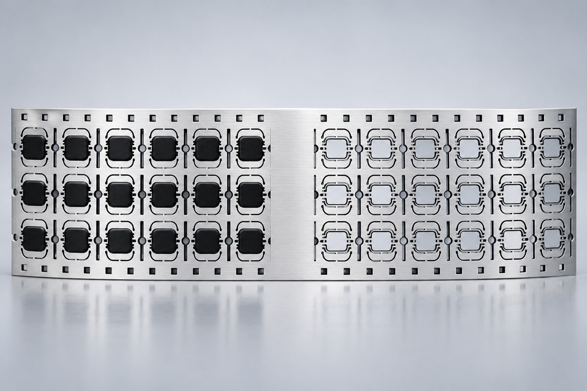 The module is only one layer in a contactless card or document construction. A lower module profile can create more room within the stack-up, but the die, antenna, adhesive, substrate and lamination process must be reviewed together. SOA6 is listed with a nominal 250 μm overall profile in the supplied product documentation. 01 / PROJECT CONSIDERATIONS Start with the complete stack-upDefine the finished construction and identify the thickness contribution of every layer. The nominal module thickness is not the finished card or inlay thickness. Confirm tolerances, local material build-up, bonding and lamination conditions using the approved drawing. 02 / PROJECT CONSIDERATIONS Compare related module formatsThe supplied March 2021 documentation lists SOA6 at 250 μm, SOA4 at 320 μm and SOA2 at 390 μm. It lists a maximum die size of 3.0 × 3.3 mm for these formats and a recommended thinned die thickness of 70 μm for SOA6. Confirm current availability, drawings and chip-specific requirements before selecting a configuration. 03 / PROJECT CONSIDERATIONS Validate the production interfaceThe source describes shared pad geometry and process compatibility with SOA2/SOA4. This is a starting point for evaluation, rather than a substitute for process qualification. Review carrier indexing, antenna attachment, bonding, handling and inspection on representative assemblies. Build a clear selection brief
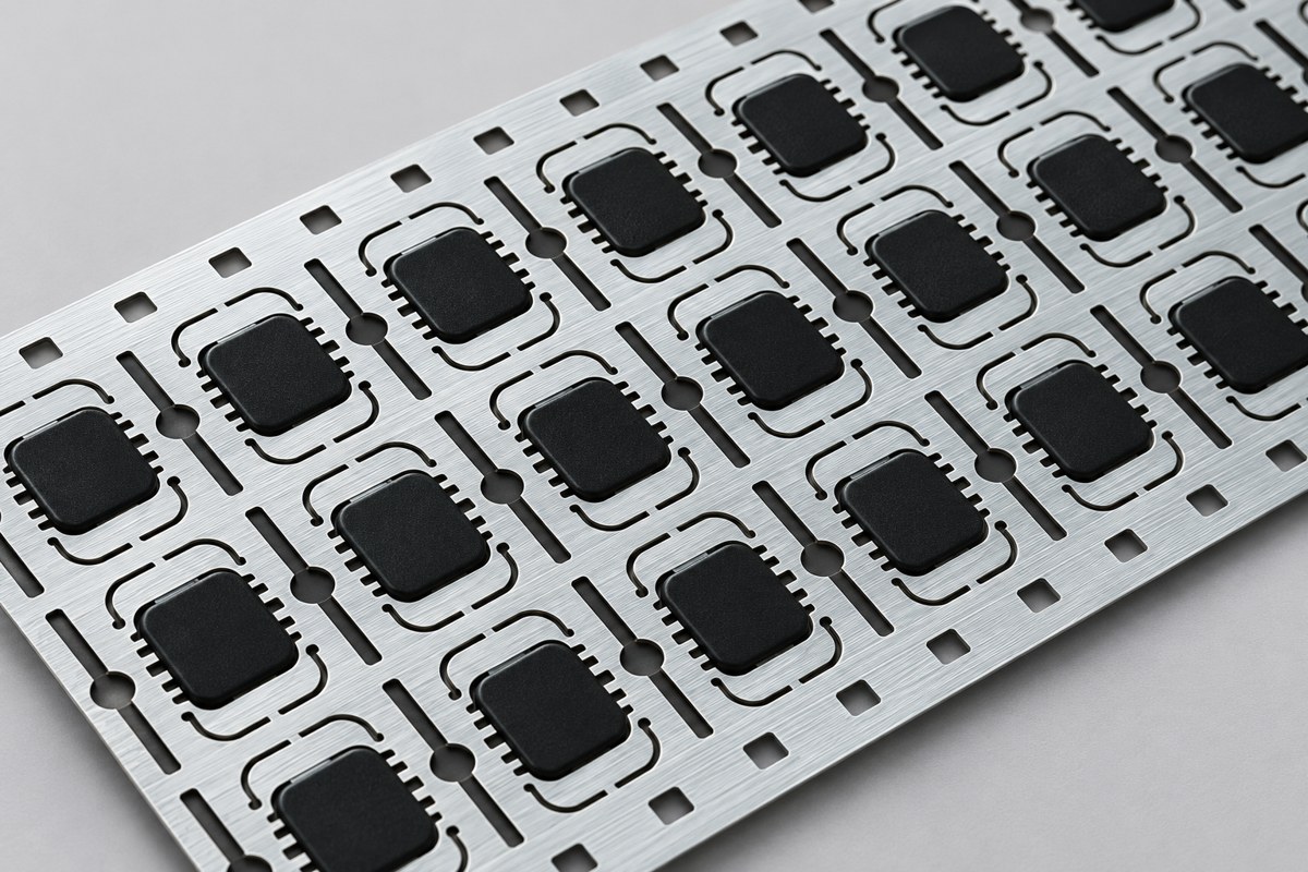 From requirements to evaluationStart with the application and an existing part, chip or reader reference where available. Review the mechanical and electronic configuration, evaluate representative samples in the intended assembly, and agree on acceptance criteria before confirming the production configuration. Explore the relevant product familiesSOA6 Ultra-Thin Contactless Modules → Share your product reference, drawings, intended application, quantity and schedule so the appropriate configuration can be discussed. Discuss your project →Product-family illustrations. Exact construction, compatibility and availability depend on the selected product configuration and approved documentation. |