|
SOA6 Ultra-Thin Contactless Modules — 250 μm PRODUCT DETAILS
ULTRA-THIN CONTACTLESS MODULES Less thickness. |
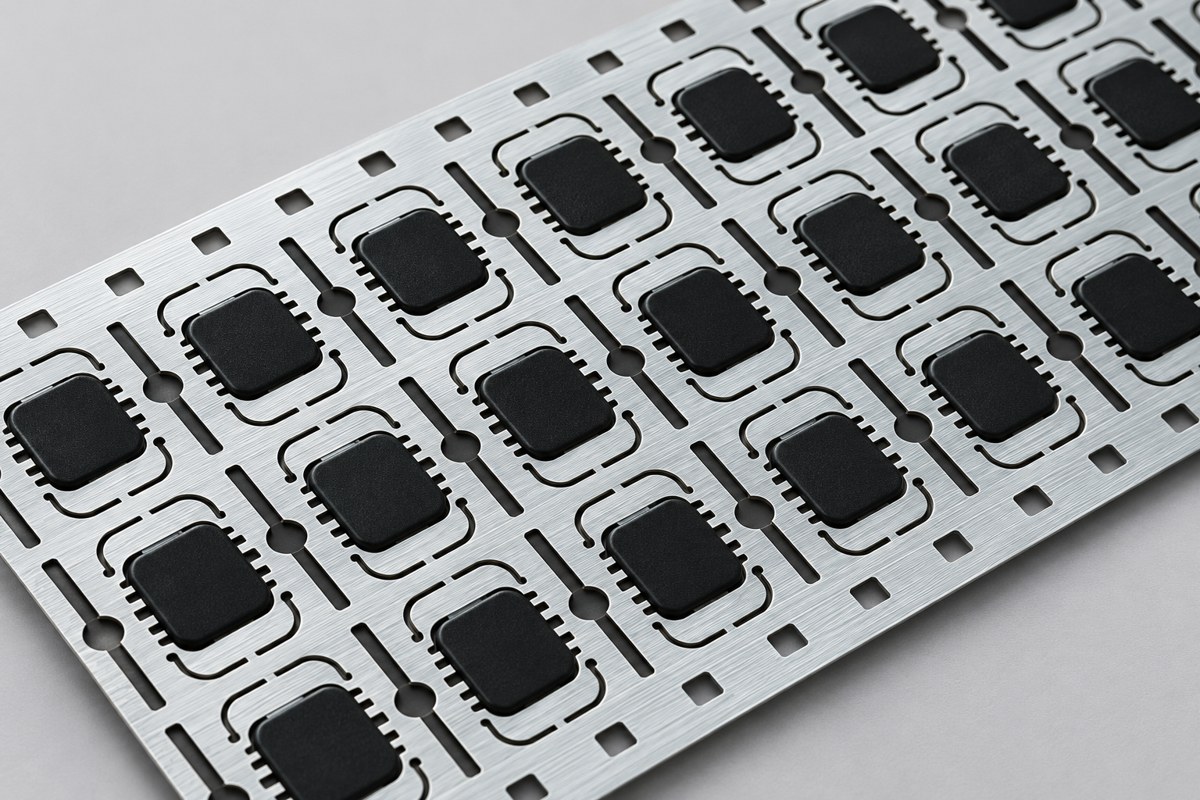
| Product model | SOA6 |
| Product type | Ultra-thin contactless smart card module |
| Nominal overall thickness | 250 μm (0.25 mm) |
| Carrier thickness | 60 μm |
| Carrier material | Copper foil with silver / nickel plating options as specified in the source documentation; confirm the selected finish |
| Maximum die size listed | 3.0 × 3.3 mm |
| Recommended thinned die thickness listed | 70 μm |
| Related module formats | SOA4: 320 μm; SOA2: 390 μm |
| Pad geometry | Described as matching SOA2 / SOA4; use the approved product drawing |
| Chip and protocol | Defined by the selected IC; confirm compatibility for the application |
03 / FAMILY COMPARISON
Choose the profile that fits the stack-up
| Module | Overall thickness | Maximum die size | Recommended thinned die thickness |
| SOA6 | 250 μm | 3.0 × 3.3 mm | 70 μm |
| SOA4 | 320 μm | 3.0 × 3.3 mm | 120 μm |
| SOA2 | 390 μm | 3.0 × 3.3 mm | 150 μm |
These values are listed in the supplied March 2021 product documentation. They are selection references; confirm current drawings, tolerances and chip-specific requirements before placing an order.
04 / APPLICATIONS
Built into a complete contactless solution
Thin contactless cards
For card constructions in which module height must fit a restricted layer stack. Coordinate the module, antenna, card materials and reader system.
Identity document inlays
Evaluate thin module integration for document and credential inlays, including inner-page constructions. Security functions and program requirements depend on the selected IC and complete document design.
Migration from existing formats
For projects reviewing a move from SOA2 or SOA4 to a lower profile. Compare pad drawings, carrier indexing, bonding, lamination and final assembly performance with representative samples.
05 / EVALUATION
Review the process before production
The supplied product documentation reports thermal-shock evaluation from −55 °C to +125 °C, using a 30 min / 1 min / 30 min sequence for 50 cycles, and damp-heat evaluation at 85 °C / 85% RH for 168 hours. It also reports gold wire bond pull and shear testing. These are reported evaluation conditions, not a continuous operating-temperature rating or a certification for every configuration. Request the applicable test report and acceptance criteria for the selected product.
| Define the electronics | IC reference, die size and thickness, antenna design and required reader / protocol compatibility |
| Confirm the mechanical interface | Module drawing, total thickness tolerance, carrier format, indexing and pad dimensions |
| Validate integration | Antenna attachment, bonding, lamination, handling and inspection under the intended process conditions |
| Agree on the order brief | Selected configuration, sample quantity, production quantity, packaging and delivery schedule |
06 / COMMON QUESTIONS
A clear starting point for your project
Is 250 μm the finished card thickness?
No. It is the nominal module profile. The complete card or inlay also includes the antenna, substrates, adhesives and other layers.
Does the module include a specific chip or protocol?
Chip functions, memory, communication protocol and security features depend on the chosen IC. Provide your chip or system reference when requesting a configuration.
Can SOA6 replace SOA2 or SOA4 directly?
The source describes shared pad dimensions and process compatibility, but the selected chip, carrier drawing and complete production process still require validation. Evaluate representative samples before changing a production configuration.
DISCUSS YOUR CONFIGURATION
Start with your card stack-up.
Send your IC reference, module drawing, target card or inlay construction, antenna connection requirements, quantity and schedule.
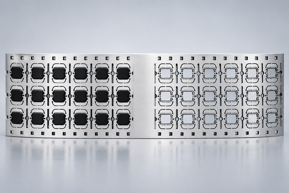
Contact HIC SMART →Studio visualizations are based on the supplied physical product reference. Exact geometry and dimensions are defined by the approved drawing.