|
DFN & QFN Semiconductor Packages Description
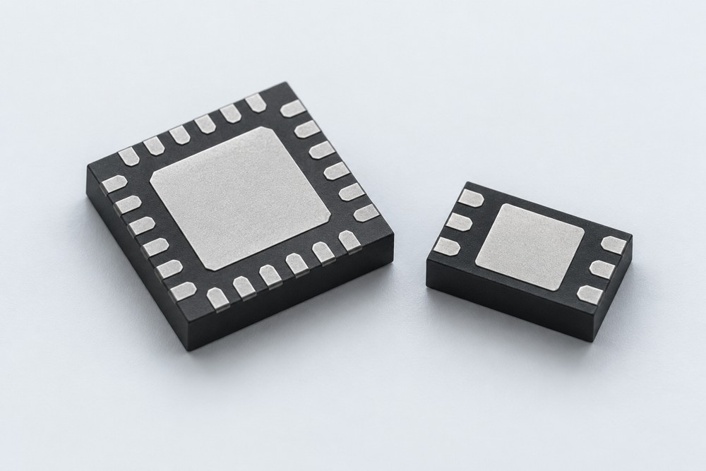
DFN and QFN are leadless surface-mount package families used to connect semiconductor devices to printed circuit boards. Their electrical terminals are located on the underside of the package. Selection starts with the device requirements and the exact package drawing, rather than the package name alone. Package architectureCompare terminal arrangement, exposed-pad geometry and body dimensions before selecting a package outline. Board integrationMatch the package drawing to the PCB land pattern and the device pin assignment. Assembly readinessReview stencil, reflow, handling and inspection requirements with the selected construction. 01 / PRODUCT OVERVIEW Understand the product familyDFN and QFN at a glanceDFN (Dual Flat No-Lead) packages typically have terminal contacts along two opposing sides. QFN (Quad Flat No-Lead) packages typically have contacts along four sides. Exposed-pad variants may provide a thermal connection to the PCB. Terminal count, pitch, body size and exposed-pad geometry depend on the specific package. Typical application contextsLeadless package families are used across analog and mixed-signal devices, interface circuits, power-management devices, sensors and connected electronics. Suitability for an application must be assessed against the selected device, package construction and required qualification criteria. Design and assembly considerationsReview the PCB land pattern, solder-mask openings, stencil design, thermal pad and reflow conditions together. Package outline and pin assignment must match the board design. DFN and QFN products should not be assumed to be footprint-compatible. 02 / APPLICATION CONTEXTS Designed into a wider systemAnalog & mixed-signalInterface circuits, signal-conditioning devices and related electronics where footprint and electrical connections must be coordinated. Power managementCompact board designs in which the exposed pad, copper layout and thermal path require particular attention. Sensors & connected devicesSpace-conscious electronic assemblies where package size, terminal layout and system requirements guide selection. 03 / CONFIGURATION GUIDE What to define before selection
05 / INTEGRATION CHECKLIST Move from requirements to evaluation01 Define the applicationIdentify the system, reader or device reference and the environment in which the product will operate. 02 Confirm the configurationReview the product drawing, electronic requirements, delivery form and any necessary application approvals. 03 Evaluate representative samplesAgree on sample quantity, integration conditions and acceptance checks before confirming the production configuration. 04 Prepare the order briefConfirm product reference, drawings, quantity, delivery schedule and any agreed inspection or personalization requirements. Product-specific review points
06 / COMMON QUESTIONS A clearer starting pointWhat is the practical difference between DFN and QFN?DFN typically places contacts on two opposing sides; QFN typically uses four sides. The names describe package families, so the actual pin count, pitch and pad geometry must come from the individual drawing. Can a DFN or QFN package be substituted directly?A similar body size does not establish compatibility. Check the IC function, pin assignment, land pattern, thermal pad and assembly requirements before considering a substitution. How should the exposed pad be handled?Use the selected device and package documentation to determine its electrical and thermal role. PCB copper, solder coverage and vias must be reviewed together with the recommended assembly process. START A PRODUCT DISCUSSION Tell us what your application needs.Please provide the IC or device reference, package drawing, target application, required quantity and schedule. Add any material, inspection or qualification requirements so the relevant product options can be reviewed. Contact HIC SMART →Original product-family illustration. Exact construction, specifications and availability depend on the selected product drawing and written configuration confirmation. |